
AOI
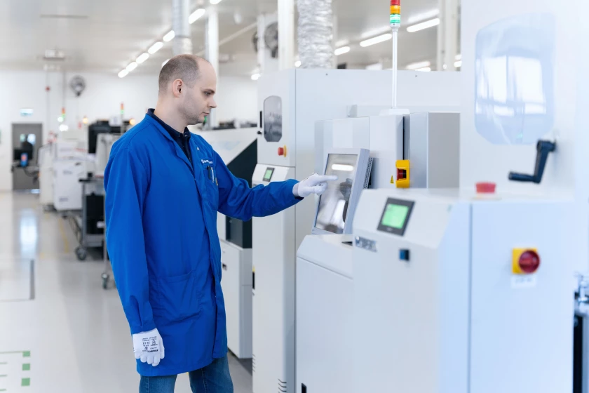
After soldering, it is crucial to check the component placement quality. Since we focus on low-mix, high-volume electronics production, automated optical inspection (AOI) suits our needs. When the AOI starts, the operator prepares it with a designated program.
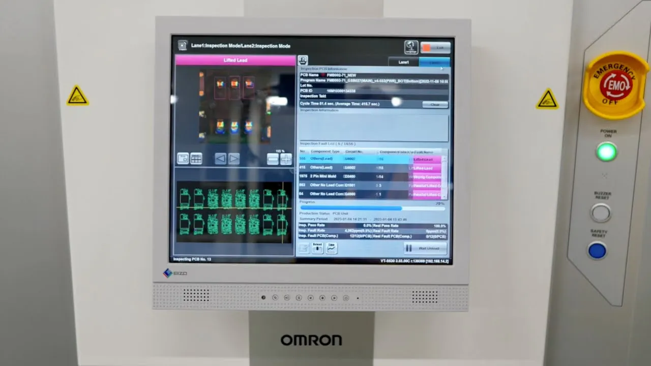
The main purpose of it is to check printed circuit board assemblies for flaws. AOI uses cameras to scan PCBAs and finds two categories of defects: catastrophic failures, such as missing components, and quality failures, like crooked fillets or skewed components.
We use an AOI machine, which has two conveyors for both sides of the PCB board. In the machine, there are sensors that detect the arrival of the PCB. Inside the machine, there is a camera that captures the whole cycle. Then the software determines if there are discrepancies. If there are no mistakes, the board enters the pass section, and if a single mistake is found, it enters the check section.
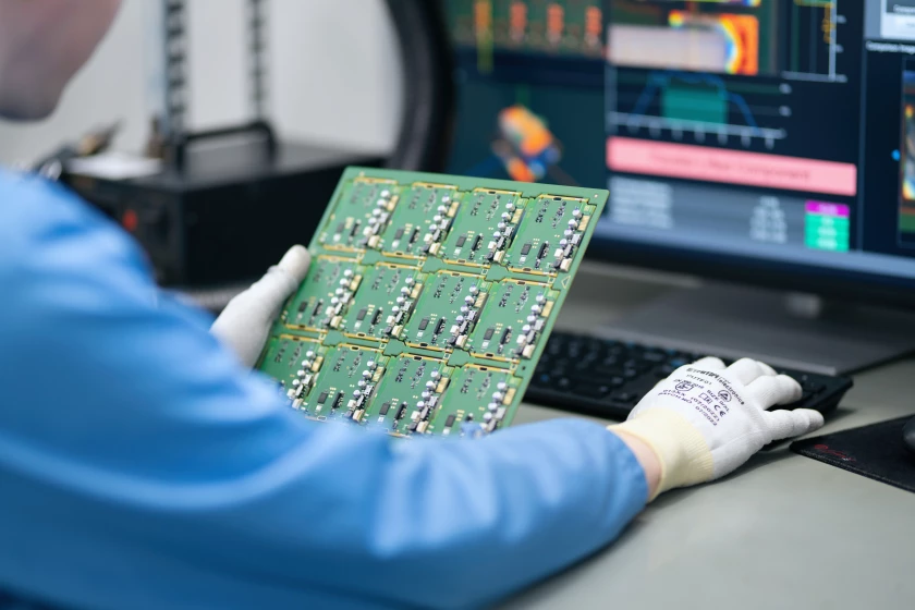
Boards that have not passed the AOI inspection are additionally checked in designated stations. An expert in AOI scans the PCBs board's data matrix and reviews photographs taken. The programme shows the intended result of the component placement. AOI specialist decides if a small amount of soldering can fix the problem or if the board needs to be relocated to a rework station. If it's a small issue, the experts solder themselves.
If incorrect flaws are discovered, AOI specialists can reprogram automatic optical inspection devices or alter currently running programmes.
![]()