
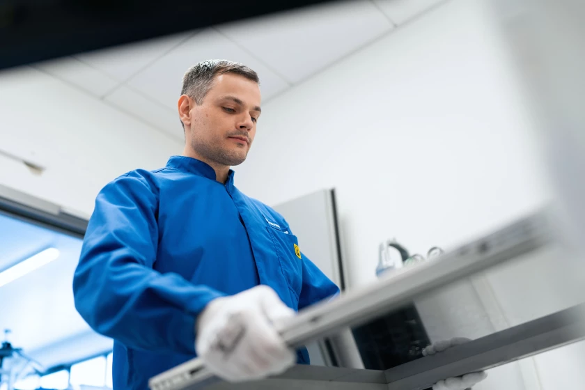
Stencil cutting
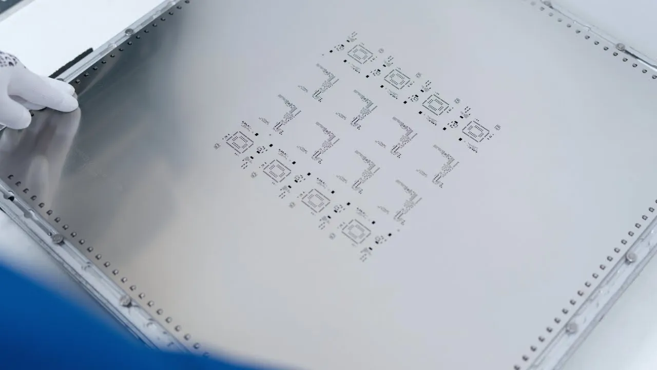
For quick solder paste application, stainless steel stencils are used. The stencil layout includes surface mount device (SMD) footprints, via which the solder paste is pressed in the screen-printing process. Since the stencil is cut according to the PCB board design, it has to be altered if any changes or improvements occur in the project. Most often, we use 100- or 120-micron stainless steel stencils to apply the right amount of solder paste to the pads.
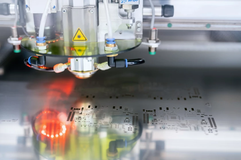
Due to the high cost of the laser equipment used to cut the stencils, electronics manufacturing companies often outsource the stencil production. To make the new product introduction stage shorter, we have a cutting laser at our facility. So, our engineers can create and cut a new stencil in-house for a new project or its improvement.
We use two types of stencil cutters. They offer high flexibility with aperture modifications, engraving logos, part numbers, or matrix codes.
Our newer edition of the laser cutter precisely uses argon gas to join two different metal sheets, allowing us to create step stencils. This enables us to develop advanced PCB board designs and improve the soldering procedure.
![]()