
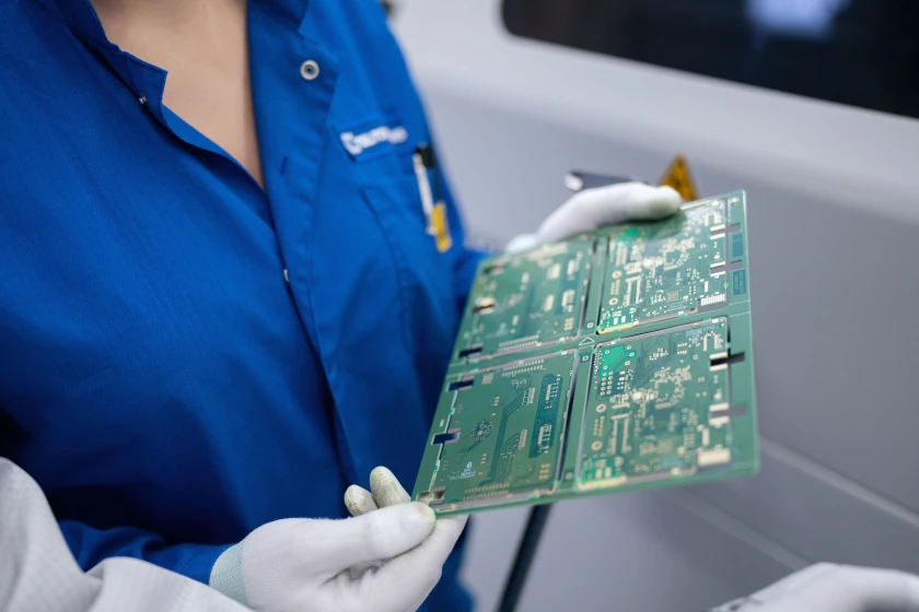
PCB Laser engraving
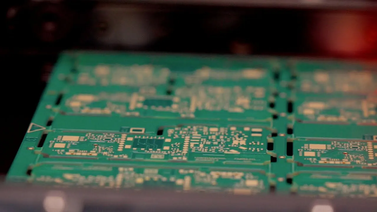
Every printed circuit board, the foundation of electronic devices, must be coded and marked to enable complete traceability and quality control throughout the electronics manufacturing process. There are several ways to mark PCBs, however, laser marking is the most efficient in our practice.
It delivers high contrast and exact marking, saves time and energy, and doesn't contaminate the PCB board panel's solder connections or circuitry.
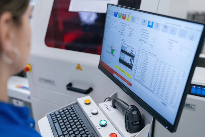
At our facility, for laser engraving of PCBs we use the CO2 marking laser. This machinery features a fiducial mark, a PCB board orientation check function, a program-controlled conveyor width adjustment, and an inbuilt inverter for double-sided marking. The option to engrave design features such as a logo is also available with this system. Additionally, we recently acquired inline lasers. They are made to mark PCB boards as they move along the assembly line, speeding up production.
By scanning the data matrix, all the manufacturing steps can be tracked, helping to assure the PCB is assembled in quality.
![]()